
Huawei Targets 2027 Density Leap with Kirin 9050 Pro unveil
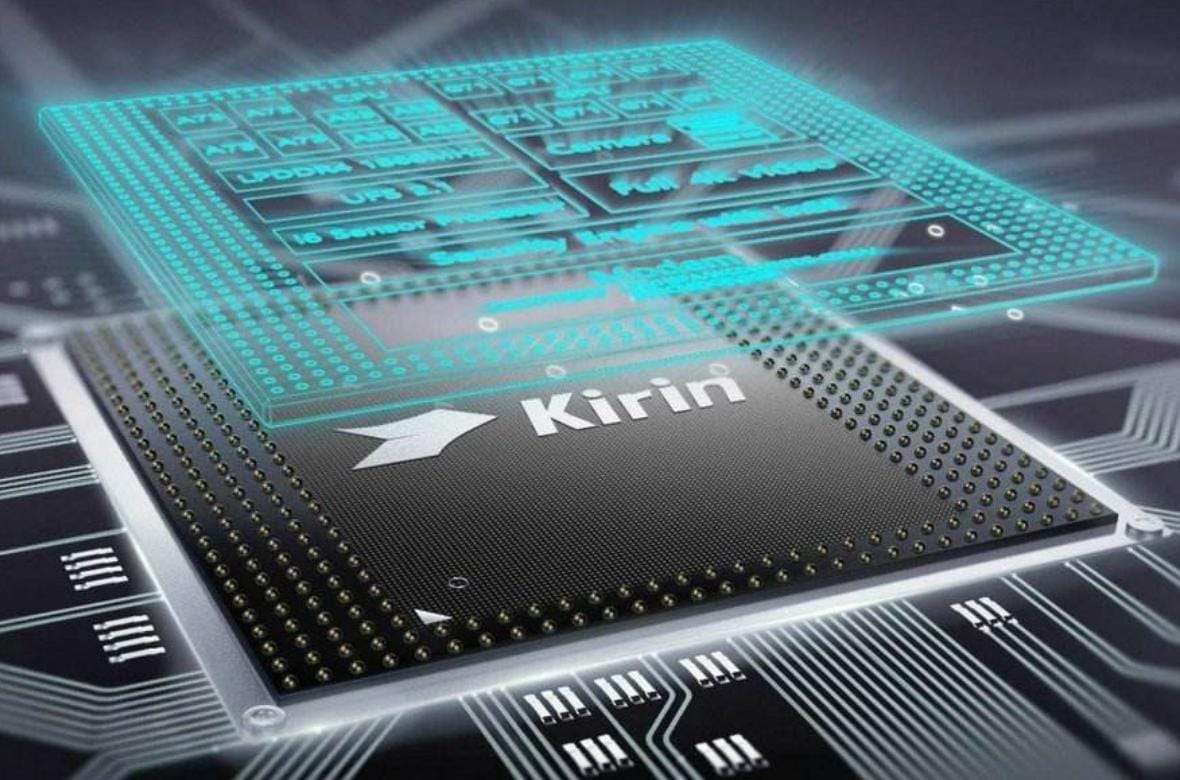
Shanghai tech briefing marks first Kirin-focused developer session in six years, as Huawei discloses a 53.5% transistor density gain and pivots its chip roadmap around "Tau Scaling" amid persistent process-node constraints.
Huawei Technologies on Thursday staged its most technically detailed Kirin chip briefing since 2019, publicly disclosing for the first time that its Kirin 9050 series achieves commercialized logic folding — a three-dimensional die-stacking architecture the company argues can sustain Moore's Law-equivalent scaling even as conventional geometric shrinkage approaches physical limits.
The event, held in Shanghai, drew immediate attention from analysts tracking China's semiconductor self-sufficiency drive. Huawei's semiconductor wireless terminal chip product management director Xu Songyu confirmed that the next-generation 2027 Kirin chip has entered the testing phase with results "meeting expectations" — a carefully worded signal that the company's domestic fabrication roadmap remains on schedule despite ongoing U.S. export controls on advanced lithography equipment.
Logic Folding Reshapes the Chip Design Playbook
The Kirin 9050 Pro is the first commercial chip built under Huawei's proprietary "Tau Scaling" framework, which replaces traditional geometric node shrinkage with what the company calls "temporal miniaturization" — compressing signal propagation latency rather than transistor physical size.
The practical architecture result: more than 50 million hybrid bonding interconnects, over 5 million effective signal connections, and a 53.5% improvement in transistor density versus the prior generation. Critically, this was achieved not by stacking pre-designed dies, but through a ground-up 3D co-design methodology where logic circuits are assigned optimal vertical positions across multiple dies from the initial design stage.
The performance payoff is substantial. The Kirin 9050 Pro's large CPU cores deliver a 41% energy-efficiency gain, while the Neural Processing Unit — built on Huawei's seventh-generation DaVinci architecture — posts a 140% performance uplift with 66% lower power consumption compared to its predecessor.
Xu noted the current hybrid bonding pitch stands at 1.5 micrometers, with a roadmap target of 1.0 micrometer by 2027. Multi-layer logic folding remains under exploration for subsequent generations.
On-Device AI Architecture Targets the 30B Parameter Frontier
Huawei is positioning the Kirin 9050 series explicitly around what it terms "Mobile Agent" use cases — smartphone applications that proactively understand user intent and execute multi-step tasks rather than responding to discrete commands.
The chip's AI subsystem deploys a dual-brain architecture: a high-capability "cerebrum" for complex reasoning and task planning, and a low-power "cerebellum" for persistent background perception. Supporting this is a 9-core, 16-thread Lingxi CPU with SMT hyper-threading, delivering a 23% multi-core performance gain, paired with Huawei's FFTS function-flow task scheduler capable of 500,000 concurrent dispatches per second at microsecond-level latency.
The headline on-device AI specification — running a 30-billion-parameter Mixture-of-Experts large language model locally — directly challenges Qualcomm's and Apple's latest flagship claims on edge AI. Huawei achieves this with under 2.5GB of incremental memory consumption, a 25% improvement in model loading speed, and a 75% reduction in memory footprint versus the previous generation. A memory compression accelerator co-optimized with HarmonyOS's Ark Engine contributes an additional average 3GB of usable RAM through a 45% compression ratio improvement.
Camera and Connectivity: ISP Parallelism and Four-SIM Debut
The imaging pipeline undergoes a structural redesign. Prior Kirin generations processed ISP and NPU image enhancement tasks serially; the Kirin 9050 series introduces a pixel-dedicated NPU embedded within the ISP itself, enabling parallel processing of 4K video quality enhancement and AI computational photography simultaneously.
Additional imaging specifications: a 200-megapixel fusion ISP with 2x pixel throughput improvement and 18EV high dynamic range support.
On connectivity, the series marks the commercial debut of four-SIM, three-standby operation via the new-generation Balong AI Modem. The Marly GPU — now on its fourth-generation architecture — delivers a 40% performance gain. Battery endurance on the Huawei Mate 90 Pro Max reaches 45 hours for long-form video and 23 hours for short-form content.
R&D Spend Hits Record, Foldable Market Share Consolidates Above 70%
Huawei Terminal BG CTO Li Xiaolong disclosed that the company invested RMB 121.4 billion (approximately US$16.9 billion) in research and development in the first half of 2026 — a record for any comparable period — representing a 25.2% year-on-year increase and an R&D intensity ratio of 25.9% of revenue. Cumulative R&D investment over the past decade reached RMB 1.382 trillion (approximately US$191.9 billion).
The figures underscore a deliberate capital allocation strategy: sustained technology investment as a primary competitive moat rather than margin expansion, a posture that differentiates Huawei from most global handset peers.
On the device front, Li confirmed cumulative foldable smartphone shipments have surpassed 20 million units. In the first half of 2026, Huawei's domestic foldable smartphone market share exceeded 70% — a dominant position that reflects both brand loyalty and a near-absence of comparably priced domestic competitors in the premium folding segment.
Since the Kirin platform's return in August 2023, cumulative shipments of Kirin-powered terminal devices have crossed 100 million units, spanning the Mate, Pura, Nova, and Enjoy product lines — a velocity that validates the commercial viability of Huawei's domestically constrained supply chain.
Impact Assessment: What the 2027 Roadmap Signals for the Semiconductor Landscape
The six-year gap between formal Kirin technical briefings was not accidental; it reflected the uncertainty created by successive U.S. sanctions targeting Huawei's access to advanced foundry services. Thursday's event marks a deliberate posture shift — from defensive opacity to measured technical transparency — suggesting internal confidence that the logic folding architecture provides a credible multi-year roadmap independent of access to sub-7nm foundry nodes.
The 1.0-micrometer hybrid bonding target for 2027 aligns with industry benchmarks set by TSMC's SoIC and Intel's Foveros Direct packaging technologies, though Huawei's manufacturing partner and node specifics remain undisclosed. Investors monitoring China's semiconductor equipment sector — particularly companies supplying advanced packaging tools — should treat the Kirin 9050 architecture disclosure as a forward demand signal.
For global handset chip vendors, the 30B MoE on-device AI benchmark and the parallelized ISP-NPU architecture set a new competitive reference point heading into 2027 product cycles.
Related Coverage:
Huawei-Qualcomm Patent Pact Signals China's Rising Royalty Power