
Huawei’s Tao’s Law V2 Bypasses EUV Constraints, Repricing China’s Chip Supply Chain
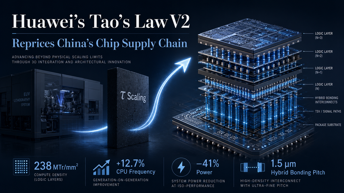
Huawei CEO of Semiconductor Division He Tingbo has published a second-generation theoretical framework—dubbed Tao's Law (τ-Law) V2—that uses logic folding and hybrid bonding to achieve advanced-node performance without EUV lithography, with the Kirin 2026 chip set for mass production in H2 2026 and benchmark specifications matching TSMC's N4P process node.
The paper, formally released July 3 on the Chinese Academy of Sciences' ChinaXiv preprint platform, marks a decisive shift from the V1 conceptual draft published May 25. Where V1 established a theoretical alternative to Moore's Law's geometric-scaling paradigm, V2 closes the loop with production-verified data: transistor density climbing 53.5% to 238 MTr/mm², CPU core frequency rising 12.7% to 3.1 GHz, and power consumption falling 41%—all achieved on mature process nodes that China's domestic foundries already operate at scale. The hybrid bonding pitch has been demonstrated at 1.5μm with overlay accuracy below 0.5μm, parameters the source material identifies as production-feasible.
Market reaction to the disclosure has been immediate. Investors are re-pricing the entire domestic semiconductor supply chain on the premise that a credible, iterative alternative to EUV-dependent scaling now exists in China, removing what had been the most structurally intractable ceiling on indigenous chip performance.
Tao's Law V2 Redefines the Scaling Metric That Has Governed Chip Design for Decades
The central intellectual contribution of V2 is the formalization of τ (tau) scaling—a four-tier mathematical framework that decomposes chip optimization across transistor, circuit, die, and system dimensions, spanning 12 orders of magnitude from picoseconds to seconds. This replaces V1's unified acceleration factor with scene-specific optimization models, giving the framework engineering precision rather than conceptual generality.
The practical implementation relies on LogicFolding, a three-dimensional topology technique that moves beyond conventional 3D stacking's function-block-level granularity to enable unit-level continuous global optimization. By vertically partitioning combinational logic, sequential logic, analog circuits, and memory into distinct stacked layers—interconnected via hybrid bonding—the architecture shortens interconnect length, suppresses parasitic parameters, and resolves the N² compute versus N bandwidth bottleneck endemic to conventional planar designs.
The roadmap is explicit: clock frequencies are projected to reach 5 GHz by 2027–2031, ultimately achieving N2P-equivalent performance. He Tingbo writes in the paper: "The era of geometric scaling has ended; the era of τ optimization is beginning."
Foundry and Advanced Packaging Players Capture the Highest Direct Revenue Exposure
The architecture's multi-layer folding structure tightly couples wafer fabrication with advanced packaging, elevating the value share of the packaging step in a way that directly benefits two categories of domestic companies.
SMIC, China's dominant logic foundry, is identified as the primary manufacturing platform for scaling Tao's Law into volume production. The logic-folding process is expected to substantially increase the per-wafer revenue of advanced-node production runs, while the Kirin 2026 ramp and subsequent node iterations should drive both capacity expansion and margin improvement at SMIC—making it the highest-beta anchor in the supply chain.
JCET Group, China's leading outsourced semiconductor assembly and test provider, is one of a small number of domestic firms capable of volume production at 1.5μm hybrid bonding pitch. As packaging value intensity rises with each architectural generation, JCET's order mix is expected to shift toward higher-margin advanced packaging, improving blended profitability.
SiEn (QingDao) Integrated Circuits, focused on 3D IC integration, is positioned as a direct beneficiary of the LogicFolding ramp given its technical alignment with multi-layer stacking architectures. Hua Hong Semiconductor, Tongxi Electronics, and Huicheng Shares are expected to capture incremental orders across specialty process and high-density packaging segments as the ecosystem matures.
Equipment Makers Face the Strongest Near-Term Order Visibility
Process innovation of this complexity creates mandatory equipment demand across deposition, etch, CMP, and cleaning—categories where Chinese suppliers have made measurable share gains over the past three years.
Piotech, the domestic leader in PECVD thin-film deposition, supplies equipment that is essential for building the multiple active layers required by the stacking architecture. The increased layer count and tighter process specifications under Tao's Law directly expand the addressable equipment budget per wafer start.
NAURA Technology Group covers etch, thin-film, and cleaning equipment across a single platform, giving it the broadest revenue exposure to any advanced-node capacity build. Its multi-category positioning means Tao's Law-driven fab expansions translate into orders across the entire product portfolio simultaneously.
Advanced Micro-Fabrication Equipment holds a critical position in TSV etch and deep-silicon etch, both of which are gating process steps for 3D vertical integration. The V2 specification—TSV critical dimension below 1.5μm—sets exacting requirements that the company's existing product line is described as meeting.
ACM Research Shanghai and Huahai Qingke address the cleaning and CMP segments respectively. Multi-layer hybrid bonding imposes exponentially higher requirements on wafer surface cleanliness and planarity, making both companies' tools non-discretionary line items in any advanced packaging capacity build.
EDA Vendors Gain Strategic Leverage as 3D-Native Design Tools Become Gating Dependencies
No architectural shift of this complexity can be commercialized without corresponding design software, and the domestic EDA sector is positioned to capture share that would otherwise flow to U.S.-headquartered incumbents subject to export controls.
Empyrean Technology, China's only full-flow EDA provider covering both analog and digital design environments, is expected to deepen its collaboration with Huawei on 3D-stacking-specific toolchains. The company's participation in process co-development for Tao's Law architectures could accelerate its penetration of advanced-node design flows—a segment where domestic share has historically been negligible.
Primarius Technologies, specializing in device modeling and circuit simulation, provides the high-accuracy parameter extraction tools that determine iteration speed and final silicon performance. Its role in the Tao's Law development cycle is expected to deepen as process nodes become more complex.
Chip Design Beneficiaries: Import Substitution Accelerates at the System Level
The performance headroom unlocked by Tao's Law extends downstream to fabless and system chip designers whose competitive positioning has been constrained by process-node disadvantages.
Centec Networks, the domestic leader in high-end Ethernet switch silicon, stands to gain disproportionately from the frequency and power improvements the new architecture enables. In data center and AI networking applications—where Chinese cloud operators are actively seeking domestic supply alternatives—a credible performance upgrade narrows the gap to Broadcom and Marvell products materially.
Montage Technology, a global supplier of memory interface chips with an established position in DDR5 register clock drivers, benefits from both the process improvement and the structural demand tailwind from AI infrastructure buildout. Memory interface chips sit at the intersection of the logic-memory re-integration thesis that V2 formalizes, making Montage a conceptual as well as operational beneficiary.
Geopolitical Context: From Rule-Follower to Rule-Setter
The strategic significance of Tao's Law V2 extends beyond individual company earnings revisions. For the past five decades, the semiconductor industry's foundational theory, technical standards, and iteration cadence were defined by U.S. and Western institutions—from Moore's Law itself to EDA tool architectures and industry benchmark methodologies. Chinese companies operated as rule-takers, optimizing within a framework they did not author.
V2 represents the first instance of a Chinese institution publishing a semiconductor scaling theory that is simultaneously original in conception, mathematically formalized, and empirically validated with production silicon. Whether the global industry ultimately converges on τ scaling as a parallel standard to Moore's Law remains to be seen, but the existence of production data from the Kirin 2026 program means the framework can no longer be dismissed as aspirational.
The roadmap through 2031—targeting N2P-equivalent performance via successive architectural iterations rather than lithography node purchases—is designed to be structurally insulated from export controls. That insulation is the most durable competitive moat the framework offers, and the one most likely to sustain the current re-rating of domestic semiconductor equities beyond a single product cycle.
Related Coverage:
Huawei Unveils New Chip Law, Promises Major Kirin Boost This Fall