
China’s Innoscience Tapped by Nvidia for AI Data Center Power Shift
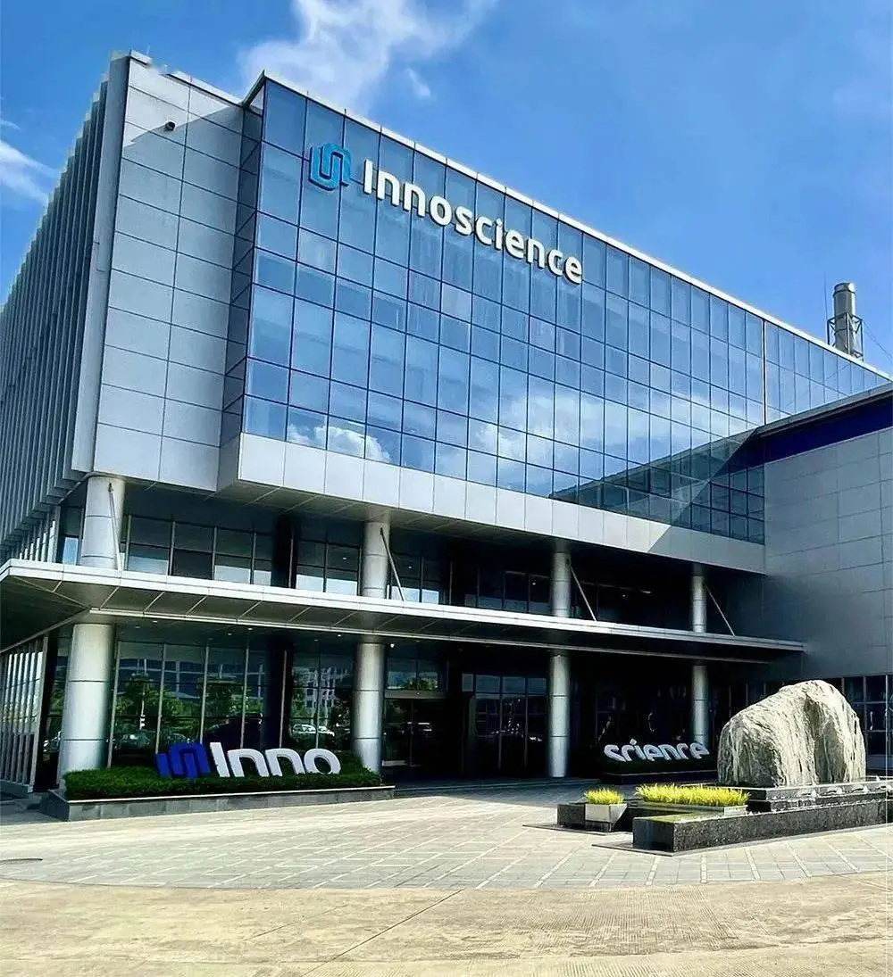
Innoscience Technology, China’s leading gallium nitride (GaN) chipmaker, has been selected by Nvidia as a key supplier for its next-generation data center power systems, a move that solidifies the company's global standing and signals China's growing prowess in the critical field of third-generation semiconductors.
The nine-year-old firm was named on August 1 as a chip supplier for Nvidia’s new 800V high-voltage direct current (DC) architecture. Innoscience joins a roster of established semiconductor giants, including Texas Instruments, Rohm, and Infineon Technologies AG, in supporting the pivotal upgrade designed to meet the surging power demands of artificial intelligence.
In a statement on its website three days later, Innoscience confirmed it would provide a full-link GaN power solution for the 800V architecture, covering the entire chain from the 800V input to the GPU. The partnership validates the Chinese company's technology and places it at the center of a hardware revolution driven by AI's insatiable appetite for computing power.
The Nvidia endorsement comes as Innoscience's financial performance gathers momentum. On August 28, the company reported first-half 2025 revenue of RMB 553 million, up 43.4% year-on-year, and achieved its first positive gross margin at 6.8%. The results, which also included the world’s first mass shipment of GaN-powered robots with a major client, point toward a potential turning point for the Hong Kong-listed firm, which already commands the largest share of the global GaN power semiconductor market.
A Bet on GaN and 8-Inch Wafers
Innoscience's ascent is rooted in a strategic bet on GaN, a third-generation semiconductor material known as a "game-changer" for its ability to deliver higher power, lower energy consumption, and smaller device sizes compared to traditional silicon. These characteristics are particularly crucial for power-hungry applications like AI data centers, where GaN can increase server rack power density by more than tenfold.
Founded in December 2015 by Dr. Luo Weiwei, a former NASA chief scientist, the company chose a challenging path from the outset. It opted for an Integrated Device Manufacturer (IDM) model, controlling design, manufacturing, and sales in-house, a departure from the capital-light fabless model common among chip startups. The goal was to overcome the key barriers to GaN adoption: high cost, inconsistent supply, and production volume.
Further amplifying the challenge, Innoscience decided to bypass the industry-standard 6-inch wafers and develop its technology directly on 8-inch wafers. While an 8-inch wafer can yield 80% more chips and reduce costs by 30%, the technical complexity increases exponentially. By November 2017, the company had established China's first 8-inch GaN-on-silicon production line, a significant breakthrough that drew industry attention.
Path to Mass Production
Despite initial difficulties in securing financing, Innoscience’s technical progress attracted crucial support. The company secured an invitation to build a third-generation semiconductor base in Suzhou, a project backed by an RMB 8 billion investment and designated as a key provincial initiative.
The firm hit a critical milestone in the summer of 2020, achieving a product yield of 92% on its 8-inch production line. This paved the way for the official launch of mass production in June 2021 at its Suzhou facility, now the world's largest GaN production base. The company's leadership was further strengthened by the appointment of Dr. Wu Jingang, a former R&D executive from Semiconductor Manufacturing International, as its CEO.
The transition to high-volume manufacturing allowed Innoscience to aggressively expand its commercial footprint. As of August 2023, its GaN chip shipments had surpassed 300 million units. The company's 2023 revenue reached RMB 593 million, and it captured a 42.4% share of the global GaN power semiconductor market, according to industry data.
Securing Key Clients and Markets
Innoscience has successfully penetrated key high-growth markets. In 2021, its VGaN product became the first GaN chip integrated into the internal power switching system of a smartphone, in a device from OPPO. It also partnered with charging brand Anker to launch a 65W all-GaN fast charger.
The company has made significant inroads into the automotive sector, with multiple products for on-board chargers and LiDAR power systems receiving AEC-Q101 automotive-grade certification between 2022 and 2023. This expansion was bolstered by a RMB 200 million personal investment from Zeng Yuqun, chairman of battery giant Contemporary Amperex Technology, which subsequently became a key customer for Innoscience's power modules.
The company’s rise has not gone unnoticed by competitors. In May 2023, US-based Efficient Power Conversion (EPC) filed a patent infringement lawsuit against Innoscience, seeking to block its products from the U.S. market. However, Innoscience successfully defended its position, leveraging its portfolio of over 700 patents to win the case.
Global Ambitions and Competitive Landscape
With its intellectual property secured, Innoscience has accelerated its global expansion, opening R&D centers and offices in Silicon Valley, Seoul, and Belgium. Founder Luo has stated her ambition is for Innoscience to become a technology leader akin to TSMC or Nvidia in the third-generation semiconductor space.
The competitive landscape remains intense. Competitor Infineon has announced that its 12-inch GaN wafers are nearing mass production. However, the market is expanding rapidly. Analysts forecast the GaN chip market will reach several billion dollars within three years and grow to tens of billions over the next decade, driven by demand from AI, electric vehicles, and robotics.
Amid a surge in overseas orders during the 2025 Chinese New Year, the company kept its facilities running with dedicated teams. "We are not chasing the time difference," a research engineer said while observing a tiny GaN wafer in the lab. "We are chasing the era."