
Huawei’s Six-Year Chip Push Tests Whether China Can Produce a Global Semiconductor Champion
When Huawei lost access to advanced global chip manufacturing after US export controls tightened in 2020, the company faced a structural problem shared across China’s semiconductor sector: how to sustain performance gains without access to the world’s most advanced lithography tools.
Six years later, Huawei is attempting to answer that question with a different optimization framework.
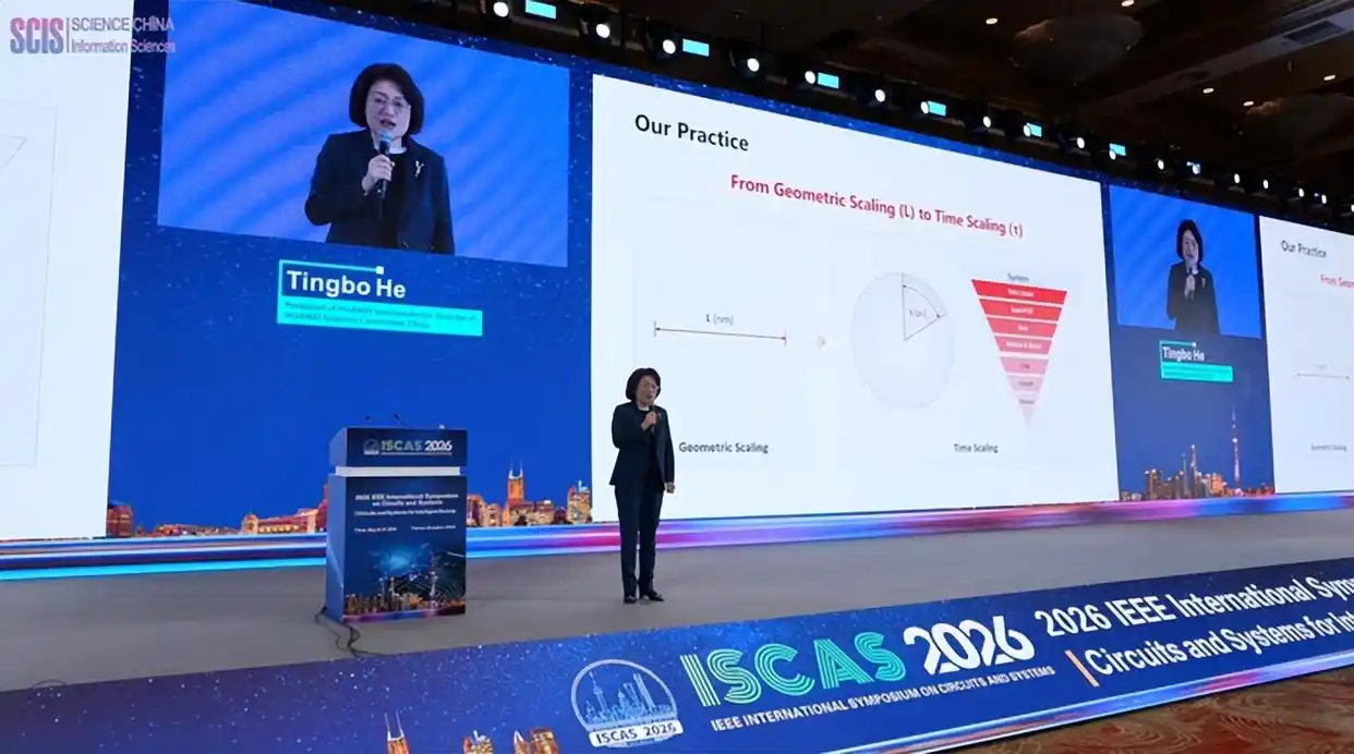
At the IEEE ISCAS conference on May 25, Semiconductor Business President Tingbo He introduced what Huawei calls the “τ (Tau) Scaling Law,” a chip design methodology that shifts semiconductor optimization away from pure geometric transistor shrinking toward system-level latency reduction and 3D architectural integration. The announcement offers the clearest articulation yet of how Huawei’s semiconductor strategy evolved under sanctions pressure between 2020 and 2026.
The timing is significant for China’s broader chip ambitions. As the economics of Moore’s Law deteriorate globally and advanced-node development costs exceed US$1 billion per generation, architectural efficiency and system-level integration are becoming increasingly important competitive variables alongside lithography leadership.
Huawei argues that transition creates an opening for China’s domestic semiconductor ecosystem.
Between 2020 and 2026, Huawei’s semiconductor teams designed and mass-produced 381 chips spanning smartphones, AI accelerators, automotive systems and infrastructure hardware, according to material presented at the conference. The company’s engineers redirected optimization efforts from geometric scaling toward what Huawei describes as “time scaling” — reducing latency constants across the computing stack, from transistor-level operations to AI workloads.
At the core of the framework is a design approach Huawei calls “Logic Folding.” Instead of relying exclusively on smaller process nodes, the technique partitions digital, analog and memory circuits into vertically stacked active layers connected through ultra-fine-pitch hybrid bonding. Huawei says the architecture shortens signal paths and reduces parasitic resistance-capacitance delays.
The company disclosed that its Kirin 2026 mobile system-on-chip achieved transistor density of 238 million transistors per square millimeter, up from 155 MTr/mm² at the same manufacturing node — a 55% increase. Huawei also reported a 41% improvement in energy efficiency and a 13% clock-frequency gain.
The AI infrastructure implications may be more commercially important.
Huawei said its Unified Bus architecture reduced remote memory access latency from tens of microseconds to roughly 100 nanoseconds, an approximately 500-fold reduction. Combined with near-package optical I/O and 3D integration, the approach is designed to address one of the AI industry’s most persistent bottlenecks: the widening gap between compute throughput and memory bandwidth.
That matters because the competitive battleground in semiconductors is increasingly shifting beyond raw transistor density.
After the slowdown of Dennard Scaling and the rising cost of sub-7nm fabrication, semiconductor competition has progressively moved toward architectural optimization, heterogeneous integration, packaging technologies and software-hardware coordination. The rise of large language models accelerated that transition by making system efficiency, interconnect performance and memory management as strategically important as pure compute power.
Huawei’s broader ecosystem strategy reflects that reality.
China’s domestic semiconductor supply chain has quietly strengthened across multiple layers during the past six years, according to the source material. Domestic foundries have stabilized 7nm-class manufacturing capabilities, while AI chip startups including Cambricon Technologies and several Chinese GPU developers have expanded local compute alternatives.
At the same time, Chinese technology groups including Huawei, Alibaba, and Baidu increasingly adopted vertically integrated hardware-software strategies similar to Apple’s ecosystem model.
The commercial relevance became more visible after DeepSeek V4 was migrated onto Huawei’s Ascend 950PR architecture. According to the source material, the development prompted multiple Chinese internet firms, including ByteDance, Alibaba and Tencent, to begin discussions with Huawei over AI chip procurement.
That shift highlights a broader strategic question facing China’s semiconductor industry in 2026: whether architectural innovation and ecosystem integration can compensate for continued constraints in advanced lithography access.
Huawei’s roadmap suggests the company believes they can. The firm projects that its τ Scaling framework could achieve transistor-density levels equivalent to 1.4nm-class chips by 2031 through 3D integration and system optimization rather than next-generation EUV-based geometric scaling.
Whether that ultimately produces a globally dominant semiconductor company remains unresolved. Chinese firms still face structural disadvantages in advanced manufacturing equipment, global software ecosystems and international customer penetration.
But the post-Moore transition may be changing the competitive rules.
As returns from pure node shrinking flatten after 7nm, the industry’s center of gravity is moving toward architecture, packaging and system-level optimization. In that environment, China’s semiconductor ecosystem no longer needs to replicate the traditional Western scaling path exactly to remain competitive in selected markets such as AI infrastructure and edge computing.
For Huawei, the past six years increasingly look less like a temporary sanctions response and more like the foundation of an alternative semiconductor development model.
Related Coverage:
What Is the Tau (τ) Scaling Law? Understanding Huawei's Alternative to Moore's Law